The polarization potential resulted from a temperature change through a series coupling effects can significantly change physical fields in piezoelectric semiconductor (PS) structures, which has been found important engineering applications in wearable electronics and temperature-related semiconductor electron devices. Using the one-dimensional multi-field coupling model for thermo-piezoelectric semiconductors, we study the effect of multiple local temperature changes on the behaviors of PS fibers. Based on the linearized current constitutive relations, we obtain the analytical solutions. For instance, a PS fiber under two local temperature changes is numerically studied. The effect of local temperature changes on the distributions of the displacement, potential, electric displacement, polarization and carrier are examined. For large temperature changes, we conduct a nonlinear analysis by COMSOL using the nonlinear current model. The numerical results show that the potential barrier and well produced by the temperature changes through a series of coupling effects depend on the magnitude of the temperature change and the thermal load position. This provides a useful theoretical guidance in the designing of devices.
Cheng Ruoran, Zhang Chunli. ANALYSIS OF THE PIEZOTRONIC EFFECT OF A PIEZOELETRIC SEMICONDUCTOR FIBER UNDER MUTIPLE LOCAL TEMPERATURE LOADINGS 1). Chinese Journal of Theoretical and Applied Mechanics[J], 2020, 52(5): 1295-1303 DOI:10.6052/0459-1879-20-128
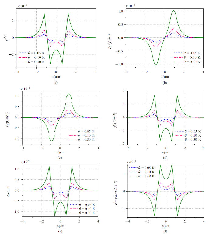
Fig.3
Distributions of (a) electric potential $\varphi$; (b) electric displacement $D_{3}$; (c) polarization $P_{3}$; (d) effective polarization charge density $\rho^P$; (e) electron concentration variation $\Delta n$; and (f) total charge for different temperature changes
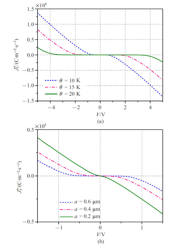
Fig.5
Electrical behavior of piezoelectric semiconductor fiber (a) $I$--$V$ cures for different temperature changes; (b) $I$--$V$ cures for different length of $a$
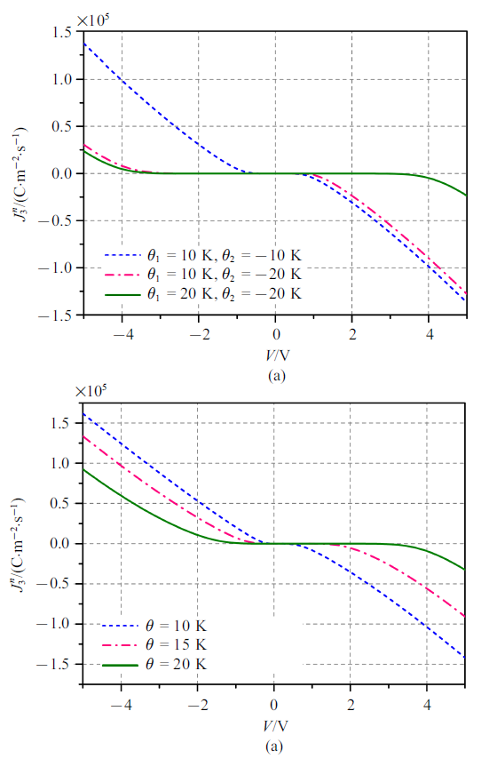
Fig.6
Electrical behavior of piezoelectric semiconductor fiber (a) $I$--$V$ cures for different $\theta_{1}$ and $-\theta_{2}$; (b) $I$--$V$ cures for different length of $a_{2}$
Flexible piezotronic devices based on RF-sputtered piezoelectric semiconductor thin films have been investigated for the first time. The dominating role of the piezotronic effect over the geometrical and piezoresistive effect in the as-fabricated devices has been confirmed and the modulation effect of the piezopotential on charge carrier transport under different strains is subsequently studied. Moreover, it is also demonstrated that the UV sensing capability of the as-fabricated thin film based piezotronic device can be tuned by the piezopotential, showing significantly enhanced sensitivity and improved reset time under tensile strain.
Enhancing the output power of a nanogenerator is essential in applications as a sustainable power source for wireless sensors and microelectronics. We report here a novel approach that greatly enhances piezoelectric power generation by introducing a p-type polymer layer on a piezoelectric semiconducting thin film. Holes at the film surface greatly reduce the piezoelectric potential screening effect caused by free electrons in a piezoelectric semiconducting material. Furthermore, additional carriers from a conducting polymer and a shift in the Fermi level help in increasing the power output. Poly(3-hexylthiophene) (P3HT) was used as a p-type polymer on piezoelectric semiconducting zinc oxide (ZnO) thin film, and phenyl-C(61)-butyric acid methyl ester (PCBM) was added to P3HT to improve carrier transport. The ZnO/P3HT:PCBM-assembled piezoelectric power generator demonstrated 18-fold enhancement in the output voltage and tripled the current, relative to a power generator with ZnO only at a strain of 0.068%. The overall output power density exceeded 0.88 W/cm(3), and the average power conversion efficiency was up to 18%. This high power generation enabled red, green, and blue light-emitting diodes to turn on after only tens of times bending the generator. This approach offers a breakthrough in realizing a high-performance flexible piezoelectric energy harvester for self-powered electronics.
GaoPX, SongJ, LiuJ, et al.
Nanowire piezoelectric nanogenerators on plastic substrates as flexible power sources for nanodevices
In this work we analyze the coupled piezoelectric and semiconductive behavior of vertically aligned ZnO nanowires under uniform compression. The screening effect on the piezoelectric field caused by the free carriers in vertically compressed zinc oxide nanowires (NWs) has been computed by means of both analytical considerations and finite element calculations. We predict that, for typical geometries and donor concentrations, the length of the NW does not significantly influence the maximum output piezopotential because the potential mainly drops across the tip, so that relatively short NWs can be sufficient for high-efficiency nanogenerators, which is an important result for wet-chemistry fabrication of low-cost, CMOS- or MEMS-compatible nanogenerators. Furthermore, simulations reveal that the dielectric surrounding the NW influences the output piezopotential, especially for low donor concentrations. Other parameters such as the applied force, the sectional area and the donor concentration have been varied in order to understand their effects on the output voltage of the nanogenerator.
BüyükköseS, Hernandez-MinguezA, VratzovB, et al.
High-frequency acoustic charge transport in GaAs nanowires
The oscillating piezoelectric fields accompanying surface acoustic waves are able to transport charge carriers in semiconductor heterostructures. Here, we demonstrate high-frequency (above 1 GHz) acoustic charge transport in GaAs-based nanowires deposited on a piezoelectric substrate. The short wavelength of the acoustic modulation, smaller than the length of the nanowire, allows the trapping of photo-generated electrons and holes at the spatially separated energy minima and maxima of conduction and valence bands, respectively, and their transport along the nanowire with a well defined acoustic velocity towards indium-doped recombination centers.
WangXD, ZhouJ, SongJH, et al.
Piezoelectric field effect transistor and nanoforce sensor based on a single ZnO nanowire
Utilizing the coupled piezoelectric and semiconducting dual properties of ZnO, we demonstrate a piezoelectric field effect transistor (PE-FET) that is composed of a ZnO nanowire (NW) (or nanobelt) bridging across two Ohmic contacts, in which the source to drain current is controlled by the bending of the NW. A possible mechanism for the PE-FET is suggested to be associated with the carrier trapping effect and the creation of a charge depletion zone under elastic deformatioin. This PE-FET has been applied as a force/pressure sensor for measuring forces in the nanonewton range and even smaller with the use of smaller NWs. An almost linear relationship between the bending force and the conductance was found at small bending regions, demonstrating the principle of nanowire-based nanoforce and nanopressure sensors.
WangZL.
Piezopotential gated nanowire devices: piezotronics and piezo-phototronics
There has been significant interest in using electronically contacted nanorod or nanotube arrays as gas sensors, whereby an adsorbate modifies either the impedance or the Fermi level of the array, enabling detection. Typically, such arrays demonstrate the I-V curves of a Schottky diode that is formed using a metal-semiconductor junction with rectifying characteristics. We show in this work that nanostructured Schottky diodes have a functionally different response, characteristic of the large electric field induced by the size scale of the array. Specifically, they are characterized by a low reverse breakdown voltage. As a result, the reverse bias current becomes a strong function of the applied voltage. In this work, for the first time, we model this unique feature by describing the enhancement effect of high aspect ratio nanostructures on the I-V characteristics of a Schottky diode. A Pt/ZnO/SiC nanostructured Schottky diode is fabricated to verify the theoretical equations presented. The gas sensing properties of the Schottky diode in reversed bias is investigated and it is shown that the theoretical calculations are in excellent agreement with measurements.
LiuY, ZhangY, YangQ, et al.
Fundamental theories of piezotronics and piezo-phototronics
The piezopotential in floating, homogeneous, quasi-1D piezo-semiconductive nanostructures under axial stress is an anti-symmetric (i.e., odd) function of force. Here, after introducing piezo-nano-devices with floating electrodes for maximum piezo-potential, we show that breaking the anti-symmetric nature of the piezopotential-force relation, for instance by using conical nanowires, can lead to better nanogenerators, piezotronic and piezophototronic devices.
ZhangCL, WangXY, ChenWQ, et al.
An analysis of the extension of a ZnO piezoelectric semiconductor nanofiber under an axial force
We have applied the perturbation theory for calculating the piezoelectric potential distribution in a nanowire (NW) as pushed by a lateral force at the tip. The analytical solution given under the first-order approximation produces a result that is within 6% from the full numerically calculated result using the finite element method. The calculation shows that the piezoelectric potential in the NW almost does not depend on the z-coordinate along the NW unless very close to the two ends, meaning that the NW can be approximately taken as a
GaoYF, WangZL.
Equilibrium potential of free charge carriers in a bent piezoelectric semiconductive nanowire
We have investigated the behavior of free charge carriers in a bent piezoelectric semiconductive nanowire under thermodynamic equilibrium conditions. For a laterally bent n-type ZnO nanowire, with the stretched side exhibiting positive piezoelectric potential and the compressed side negative piezoelectric potential, the conduction band electrons tend to accumulate at the positive side. The positive side is thus partially screened by free charge carriers while the negative side of the piezoelectric potential preserves as long as the donor concentration is not too high. For a typical ZnO nanowire with diameter 50 nm, length 600 nm, donor concentration N(D) = 1 x 10(17) cm(-3) under a bending force of 80 nN, the potential in the positive side is <0.05 V and is approximately -0.3 V at the negative side. The theoretical results support the mechanism proposed for a piezoelectric nanogenerator. Degeneracy in the positive side of the nanowire is significant, but the temperature dependence of the potential profile is weak for the temperature range of 100-400 K.
FanSQ, LiangYX, XieJM, et al.
Exact solutions to the electromechanical quantities inside a statically-bent circular ZnO nanowire by taking into account both the piezoelectric property and the semiconducting performance: Part I--Linearized analysis
Nano Energy, 2017,40:82-87
DaiXY, ZhuF, QianZH, et al.
Electric potential and carrier distribution in a piezoelectric semiconductor nanowire in time-harmonic bending vibration
Nano Energy, 2018,43:22-28
YangGY, DuJK, WangJ, et al.
Electromechanical fields in a nonuniform piezoelectric semiconductor rod
Journal of Mechanics of Materials and Structures, 2018,13(1):103-120
An analysis of PN junctions in piezoelectric semiconductors
2017
Piezopotential in a bended composite fiber made of a semiconductive core and of two piezoelectric layers with opposite polarities
2018
Piezotronic effects in the extension of a composite fiber of piezoelectric dielectrics and nonpiezoelectric semiconductors
2018
Extension of a piezoelectric semiconductor fiber with consideration of electrical nonlinearity
2018
Extensional vibration characteristics and screening of polarization charges in a ZnO piezoelectric semiconductor nanofiber
2018
Transient extensional vibration in a ZnO piezoelectric semiconductor nanofiber under a suddenly applied end force
2018
Electrostatic potential in a bent piezoelectric nanowire. The fundamental theory of nanogenerator and nanopiezotronics
2007
Equilibrium potential of free charge carriers in a bent piezoelectric semiconductive nanowire
2009
Exact solutions to the electromechanical quantities inside a statically-bent circular ZnO nanowire by taking into account both the piezoelectric property and the semiconducting performance: Part I--Linearized analysis
2017
Electric potential and carrier distribution in a piezoelectric semiconductor nanowire in time-harmonic bending vibration
2018
Electromechanical fields in a nonuniform piezoelectric semiconductor rod


